📖 Read more: Nanopigment Sensor: Changes Color Based on pH in Seconds
⚡ The Problem: Why Electrons Are No Longer Enough
Since the 1960s, electronic chips have relied on the same fundamental architectural model: electrical signals traveling through copper or aluminum conductors to transfer data between transistors, memory, and the processor. This approach worked brilliantly for decades — but today it has reached a dead end.
As transistors shrink to sizes below 3 nanometers, electrical signals face ever-increasing resistance. Every bit passing through a copper wire generates heat, which must be dissipated by energy-hungry cooling systems. In a modern data center, nearly 40% of total energy is spent solely on cooling. With Artificial Intelligence demanding ever more computational resources, this model is becoming unsustainable — both economically and environmentally.
The solution engineers have been seeking for years is simple in concept but extremely difficult to implement: replacing electrons with photons inside the chip itself. Photons travel at the speed of light, generate no heat, and can carry far more data simultaneously. The only thing missing was a light source small enough and energy-efficient enough to be integrated into a microchip.
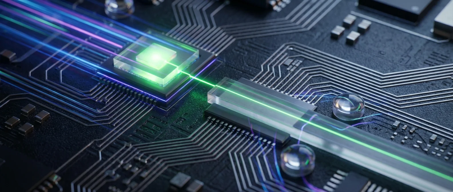
🔬 The Discovery: Nanolaser on Semiconductor Membrane
That is exactly what the team of Professor Jesper Mørk at DTU Electro achieved, in collaboration with researchers Meng Xiong and Yi Yu. Their invention, published in the journal Science Advances in February 2026, is a nanolaser built on a semiconductor membrane — a structure that breaks the traditional limits of how small a laser can be.
At the heart of the technology is a nanocavity — a light-trapping structure designed by the team of Professor Ole Sigmund at DTU Construct. This cavity concentrates light in a region so small that, until recently, it was considered physically impossible. It surpasses what physicists call the “diffraction limit” — a fundamental barrier that determines how small a field of light can get in dielectric materials.
When the researchers illuminate the laser with a beam of light, both photons and electrons concentrate in a microscopic region. This allows the laser to operate at room temperature with unusually low energy consumption — a critical feature for practical application in commercial chips.
💡 Why This Is Revolutionary
DTU's nanolaser breaks the “diffraction limit” — a physical barrier that until recently was considered insurmountable without the use of metals (which absorb light and reduce efficiency). The nanocavity traps light in a space smaller than a cell, using exclusively dielectric materials. Thousands of such nanolasers can be placed on a single microchip, replacing electrical signals with optical ones — with virtually no energy loss.
📊 The Numbers That Change Everything
Professor Mørk estimates that nanolasers can cut in half the energy consumption of computers. And this is not an arbitrary number — it stems from the near-zero energy loss during optical signal transmission, compared to the significant resistance and thermal loss in a chip's electrical wires.
The significance of these numbers is understood only at scale. Global data centers currently consume more than 400 TWh of electricity annually — more than many entire countries. A 50% reduction in energy consumption doesn't just mean lower bills: it means millions of tons fewer CO₂ emissions and a drastic reduction in the need for cooling water, which is already an environmental time bomb.
📖 Read more: 3D Printing with Sound Creates Micro-Devices
🌐 Photonic Interconnects: The Architecture of the Future
The idea of photonic computing is not new. The internet already uses photons in optical fibers for long-distance data transfer. But inside computers, data is still transferred electrically — creating a bottleneck at the point of electrical-to-optical signal conversion.
The solution is on-chip optical interconnects — photonic circuits integrated directly into the processor. Instead of data traveling as electrons through copper conductors, they are converted into light pulses that move through silicon waveguides. The company Ayar Labs, an MIT spin-off, has already developed optoelectronic chips that reduce chip-to-chip communication energy consumption by 95%.
In parallel, researchers at the University of Florida built a photonic chip (photonic Joint Transform Correlator — pJTC) that replaces electrical AI neural networks with optical circuits. Using Fresnel lenses etched in silicon and a spectral multiplexing technique — meaning data processing in multiple colors of light simultaneously — they achieved 98% accuracy in handwriting recognition, with energy efficiency reaching 305 trillion operations per second per watt.
“The nanolaser opens the possibility of creating a new generation of components that combine high performance with minimal size. It can be applied in computing, where extremely small and energy-efficient lasers can reduce energy consumption, or in developing biosensors, where extreme light concentration enables high-resolution imaging.”
🏥 Beyond Computers: Sensors and Health
Nanolaser technology is not limited to computing. The extreme concentration of light at the nanoscale enables the creation of exceptionally sensitive biosensors, capable of detecting individual molecules or disease markers in a minimal blood sample. In medical imaging, nanolasers could offer much higher resolution than current systems, opening new avenues in the diagnosis of cancer, neurodegenerative diseases, and infections.
At the network level, integrating nanolasers into smartphones would mean devices with dramatically longer battery life and faster communication. 6G mobile networks, expected after 2030, will require precisely this type of photonic components to operate at the enormous speeds they promise.
⏳ The Challenges That Remain
Despite the excitement, the technology is not yet ready for mass production. The biggest obstacle is electrical pumping: DTU's nanolaser is currently powered optically — meaning it needs an external light source to operate. Converting to an electrical pump, so the laser is activated directly from the chip's electrical circuit, is the next major challenge.
Additionally, integrating thousands of nanolasers into a chip without errors requires extremely precise manufacturing processes in state-of-the-art cleanrooms. The prototype was manufactured at DTU Nanolab, one of the most advanced nanotechnology laboratories in Europe. Scaling to industrial production will require close collaboration with semiconductor manufacturers.
The researchers estimate that the remaining technical challenges can be overcome within 5 to 10 years. If that happens, photonic chips will perhaps represent the biggest change in computer architecture since the invention of the transistor.
🔮 A Digital Future Powered by Light
DTU's invention is not merely another laboratory achievement. It is part of a global research wave aimed at fundamentally restructuring how we process information. From photonic neural networks replacing electronic ones, to optical circuits that will power the quantum networks of the future, the transition from electrons to photons now seems inevitable.
The real question is not whether this transition will happen, but how quickly. With companies like NVIDIA already using optical elements in some parts of their AI chips, and with universities in Denmark, the USA, and Switzerland breaking physical limits one by one, the era of photonic computing is approaching. And with it, a digital world that is faster, cooler, and far more friendly to the planet.
📚 Sources
- 🔗 Phys.org — Nanolaser on a chip could cut computer energy use in half (Feb 2026)
- 🔗 Science Advances — A nanolaser with extreme dielectric confinement (Xiong et al., 2025)
- 🔗 Phys.org — Semiconductor nanolasers enable ultra-efficient optical technologies (2025)
- 🔗 New Atlas — This chip uses light to supercharge AI and cut energy use (2025)
- 🔗 New Atlas — Ayar Labs optoelectronic chips reduce chip-to-chip energy 95% (2018)